The advent of 3D semiconductor packaging has transformed chip design, delivering unprecedented performance and efficiency through the vertical stacking of circuit layers. However, this breakthrough also presents critical challenges, including managing heat dissipation and ensuring precise layer alignment. These challenges demand innovative approaches that leverage cutting-edge materials and techniques to maintain functionality under increasingly complex designs. Erik Hosler, a recognized innovator in semiconductor technology, identifies advanced materials as key to addressing these obstacles, recognizing their crucial role in enhancing the reliability, scalability and overall success of 3D integration.
Tackling Heat Dissipation with Thermal Interface Materials
As chips become more densely packed, heat dissipation has emerged as a primary concern. Without efficient cooling, hotspots can damage components and shorten device lifespans. Thermal interface materials (TIMs) are specifically engineered to transfer heat between layers and away from critical areas. These materials, such as phase-change TIMs, improve thermal conductivity while maintaining structural integrity, ensuring that high-performance chips operate reliably under demanding conditions.
Enhancing Layer Alignment with Low-k Dielectrics
Precise layer alignment is essential for the seamless functionality of stacked chips. Low-k dielectrics, which feature reduced dielectric constants, minimize electrical interference between layers while enhancing signal integrity. By providing improved insulation and alignment accuracy, these materials support faster data transfer and lower power consumption, which is crucial for applications like AI and cloud computing.
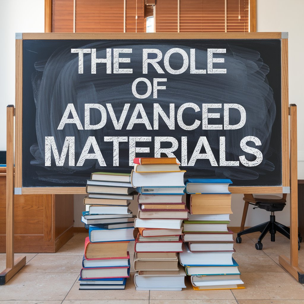
Innovations Driving 3D Integration Forward
The semiconductor industry’s evolution depends on continuous innovation to meet rising demands for performance and efficiency. Advanced materials have become indispensable in addressing the unique challenges posed by 3D integration, driving progress in chip design and functionality.
Erik Hosler explains, “Modern society is built on CMOS technology, but as we push the boundaries of what these devices can do, we must innovate within the CMOS framework to continue driving performance, efficiency and integration.” The development of novel materials tailored for 3D packaging exemplifies this commitment to innovation, enabling solutions to the complex challenges of advanced chip design.
The integration of advanced materials like thermal interface materials and low-k dielectrics is transforming 3D semiconductor packaging, addressing critical issues such as heat dissipation and layer alignment. These innovations not only ensure the reliability and performance of next-generation chips but also pave the way for new advancements in high-performance computing and AI. As the industry continues to innovate, advanced materials will remain central to overcoming the challenges of 3D integration and driving the future of semiconductor technology.